

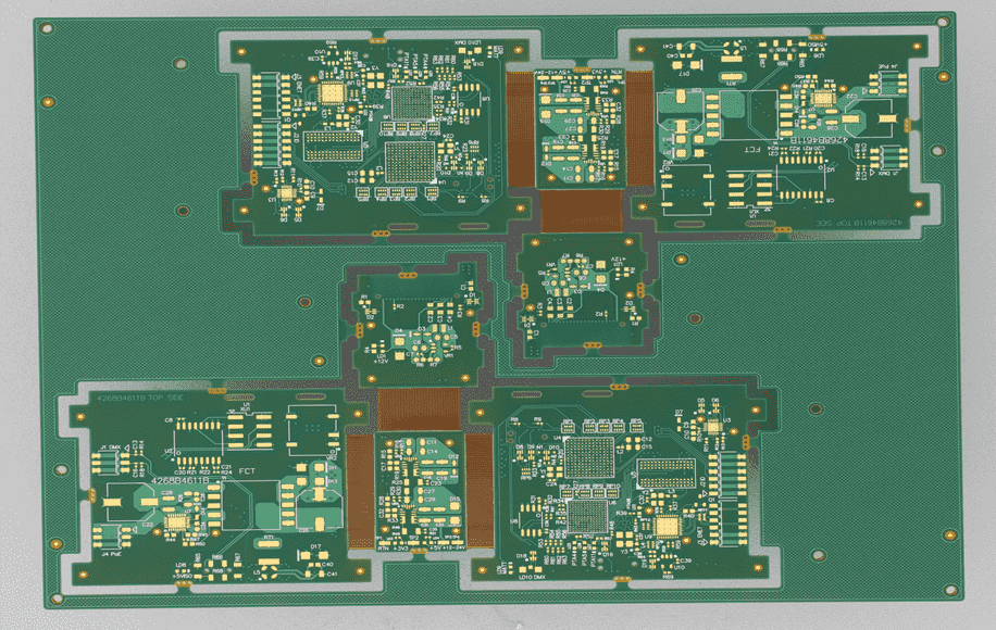
Stream PCB is a leading manufacturer specializing in all types of PCBs. We are well-recognized in the electronics industry as experts in multilayer PCB manufacturing. Our offerings include rigid, rigid-flex, and flex multilayer PCBs, as well as HDI multilayer boards.
The electronic industry utilizes various types of PCBs with multiple layers, which include:
For simple circuits, a single-layer PCB is often sufficient. Whether the circuit uses through-hole components or surface-mount devices (SMD), the single-sided board typically has copper traces on only one layer. For through-hole components, the bottom layer carries the copper traces, while for SMDs, the upper layer does.
As circuit complexity increases, a single layer is no longer enough. In double-layer PCBs, designers need copper traces on both the top and bottom layers. These boards may have vias connecting the two layers as needed. Both through-hole and SMD components are used in double-layer boards.
As a multi-layer PCB manufacturer, Stream PCB begins with a core material, typically FR4, which provides rigidity to the board. Copper cladding is attached to both sides of the core using epoxy resin. Each additional layer is built up with prepreg, which acts as an insulation and dielectric material, along with copper cladding to form the stackup. The thickness of the prepreg and copper cladding in each layer is adjusted to achieve the final board thickness.
The copper cladding in each layer undergoes processes such as photo-imaging, etching, and drilling, which are necessary for creating the vias.
The top and bottom layers of the board are subjected to solder resist printing, surface finishing, and legend printing before the board proceeds to the assembly stage.
For more details on Stream PCB multi-layer boards, please contact us today or visit our contact page.


© All Copyright 2025 by streampcb.com