What is a Printed Circuit Board (PCB)? A Beginner's Guide

The devices we use every day, from smartphones to washing machines, all rely on one crucial component: the printed circuit board (PCB). These electronic heartbeats make our technology function smoothly and efficiently. Imagine flipping a switch on your favorite gadget and, without a second thought, it turns on instantly. The magic behind that instantaneous response? A PCB.

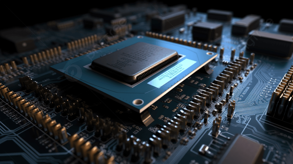
At its core, a PCB serves as a common platform for electronic components. It connects them together, ensuring they communicate effectively while powering your devices.

Streampcb Printed Circuit Board (PCB)

Understanding the Components of a PCB

The Substrate
Every PCB starts with a substrate, which acts as the base material. Common substrate materials include:
  • FR-4 (Glass Epoxy): The most popular choice, making up nearly 80% of the market.
  • CEM-1: When a lighter weight is needed, it’s often used for less complex circuits.
  • Polyimide: Valuable in high-temperature or flexible applications, though it holds a smaller market share at 10%.
Selecting the right substrate ensures durability and performance.
Conductors and Traces

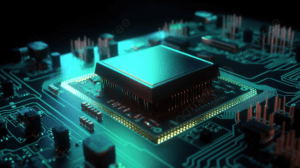
Copper is the heart of PCB conductors. These metal traces carry electrical signals and power. Trace width is vital because it affects how much current a trace can handle. For example, a wider trace can carry more current but takes up more space. This balance is key for efficient design.

Surface Mount Devices (SMDs) and Through-Hole Components
  • SMDs are placed and soldered directly onto the PCB’s surface. They occupy less space and offer higher functionality.
  • Through-Hole Components are inserted into holes and soldered on the opposite side. They provide a strong mechanical bond but require more board space.
Choosing between SMDs and through-hole components depends on the design requirements and specific application needs.

The PCB Design Process: From Schematic to Finished Product

Schematic Capture

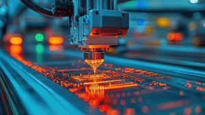
The foundation of every PCB design begins with schematic capture. This involves mapping out electronic circuits using specialized software. Accurate schematics are crucial, as they lay the foundation for the entire PCB. Popular design software includes:

  • Eagle
  • Altium Designer
  • KiCAD
PCB Layout
After capturing the schematic, the next step is PCB layout. This phase involves positioning components while considering:
  • Signal Integrity: Ensuring signals travel without loss or interference.
  • Thermal Management: Making sure the PCB can dissipate heat efficiently.
Good layout practices lead to a functioning and reliable PCB.
Manufacturing Process
The manufacturing of a PCB involves several steps, including:
  • Etching: Removing unwanted copper.
  • Drilling: Creating holes for components.
  • Soldering: Securing components onto the PCB.
For a visual overview, check out this PCB manufacturing video.

Types of PCBs and Their Applications

Single-Sided vs. Double-Sided vs. Multilayer PCBs
  • Single-Sided PCBs: Components are placed on one side only. Commonly used in basic electronics like calculators.
  • Double-Sided PCBs: Components on both sides allow for greater complexity. Found in devices like TVs.
  • Multilayer PCBs: Multiple layers allow for significant complexity and high-density applications, used in computers and smartphones.
Rigid vs. Flexible PCBs

Rigid PCBs are made from stiff materials for consistent support. Flexible PCBs, on the other hand, can bend and fold, ideal for tight spaces like in wearables. Each has its own set of advantages:

  • Rigid: Strong and dependable.
  • Flexible: Space-efficient and lightweight.
High-Frequency PCBs

High-frequency PCBs are designed specifically for applications in telecommunications and high-speed electronics. These boards require careful consideration of factors like trace width and dielectric material to handle rapid signal transmission.

Common Challenges in PCB Design and How to Overcome Them

Insufficient Clearance Between Traces

If traces are too close, it can lead to short circuits. Always ensure proper clearance for safety and performance.

Poor Thermal Management

Heat is a silent killer for PCBs. Poor design can lead to overheating, with studies showing that up to 35% of PCB failures are heat-related. Use thermal vias and appropriate materials to combat this issue.

Incorrect Component Placement

Placing components carelessly can disrupt signal integrity. Best practices include:

  • Group similar components.
  • Follow design rules for layout.
Streampcb Printed Circuit Board (PCB)

PCB Design Software and Tools

Popular PCB Design Software

Several software options streamline the design process. Each has unique features:

  • Eagle: Great for beginners, user-friendly interface.
  • Altium Designer: Advanced features for professional use.
  • KiCAD: Open-source and free, perfect for hobbyists.
Essential Tools for PCB Assembly and Testing

Once designed, essential tools include:

  • Soldering Iron: For assembling components.
  • Multimeter: To test voltage and continuity.
Resources for Learning PCB Design

Many online platforms offer courses and tutorials, such as Coursera, Udemy, and dedicated maker communities. Engaging with these resources helps foster skills and knowledge.

Conclusion: Key Takeaways and Future Trends in PCB Technology

In summary, PCBs are the backbone of modern electronics. Understanding their components, design process, types, and common pitfalls can empower enthusiasts and professionals alike.

Looking forward, trends like flexible circuits and 3D PCBs are on the rise, opening new possibilities in design and application.

Explore the fascinating world of PCB design and consider taking the first step in creating your own circuit boards. The future of electronics is in your hands!