
Free PCB Design 2-4 Layers
We will Design your PCB for FREE! Located right in the center of Silicon Valley!
Must be 2 or 4 layers and < 30 square inches
Please allow 5-7 days for a complex design
As long as we are manufacturing your board, we will provide you with the Gerber files and other related files for your records.
Stream PCB
Stream PCB Experiences & Strengths:
High-Speed PCB Design
FPGA Design
HDI Design
Multi-Layer Design
Mixed Signal Design
Blind/Buried Via Design
TDR Traces
Length-Matched Traces
Fine Pitch BGA
Constraint Manager
DFM
DFT
DFA
Customer Specific Requests
IPC CID (Certified Interconnect Designer)
Stream PCB Design Capabilities:
- High Layer Count PCB
- Blind, Buried, and Micro Via
- Mixed-Signal Design
- High-Power Circuit Design
- High-Speed Design
- High-Density Design
- Micro-BGA and BGA
- Controlled Impedance for Single Ended and Differential
- Matched Length Traces
- EMI/EMC Compliance
- Embedded Resistor
- HDI Technology
- COB
- Flex Design
- Rigid Flex Design
- MCM
- RF Design
Stream PCB Design Verification Capabilities:
- DFM & DFT
- IPC & Mil Standard
- EMC/EMI
- High-Speed Rules
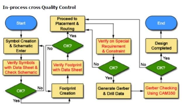
- Gerber Checking using CAM Tool
- In-Process Cross QC
Stream PCB Design Deliverables:
- Fabrication Drawings
- Assembly Drawings
- Gerber Data
- Drill Data
- Design Database
Design Tools used at Stream PCB:
- Mentor Graphics – PADS
- Altium Designer
- Eagle
- Cam 350


Inputs Required for PCB Design
- Schematic (soft copy/hand drawn)
- Bill Of Material along with manufacturing part number
- Mechanical drawing/dimensions
- Critical component placement
- Keep-out area
- Product specifications
- Environment where the PCB will be installed
Lead time
- We confirm the lead time once we have received and reviewed all the required data.
- Simple boards are typically completed within 2-3 working days.
- Moderately complicated boards take around 5-7 working days.
- High-density or complex boards usually require 10-15 working days.
Why Choose Stream PCB?
Stream PCB Technical Expertise
With an experience of more than 20+years in the industry, we possess hands-on skills in high speed, high density and high layer count PCB design.
Innovative Thinking
Stringent Protocols
Quality Assurance
Passion for Our Work
Business Engagement
FAQ's
If I do not have a soft copy of the schematic?
We prefer a soft copy of the schematic for easy extraction of the netlist, which reduces lead time. However, we can also accept hand-drawn schematics, though this may increase the lead time.
Is it necessary to provide a BOM along with the schematic?
Yes, a Bill of Materials (BOM) is necessary to determine footprints for component placement. We ensure your data is secure with us, and if needed, we are happy to sign an NDA.
What is your lead time for a quote?
We provide a quote after receiving and reviewing your inputs. If all information is provided according to your requirements, we will send the quote within 12 hours.
Do you handle mechanical or housing restrictions?
Yes, we do. To address these, we require detailed drawings or DXF files from you.
What are the alternatives if the design doesn’t fit the given size?
Our engineers will work with you at each stage of the design process. If there are issues, we will help revise your design parameters accordingly.
Do you use Auto-Routing?
We use Auto-Routing to assess the feasibility of PCB routing and to verify if the layout fits within the specified size. For the most part, we rely on manual placement and routing based on the circuit's flow. However, we manually handle the routing of DDR buses, differential pairs, and matched impedance traces.
What are your check points for design review?
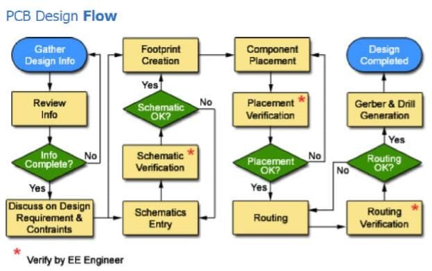
We review the design at each stage. For more details, refer to our PCB design flow chart.
Do you follow DFM (Design for Manufacturability)?
Yes, our design team works closely with the FAB team, ensuring standard DFM methods are followed.
Do you consider manual/auto assembly restrictions?
Yes, we use footprints that accommodate both manual and auto assembly. Our internal assembly team ensures this process runs smoothly.
What are the charges for revisions/modifications?
We don’t charge extra for minor changes, but major modifications may incur charges. Estimates are provided after reviewing the changes.
What if we need to cancel the order due to revisions?
If you cancel the order after revisions, you will still be required to pay for the work done.
Do you reverse engineer bare PCBs?
We can reverse engineer simple PCBs along with their schematic. We can confirm this after receiving the necessary inputs from you.
Do you take on new ideas or concept projects?
Stream PCB specializes in PCB design, fabrication, assembly, and component procurement, and does not engage in new idea or concept project development.
To get in touch with our Business Development team or to request more information about PCB layout or design services, please email us at sales@streampcb.com or call us at 1 408-982-5851.


