Assembly Reliability

Ensuring Reliable PCB Assembly: Key Challenges and Their Significance

As PCBs grow in complexity, with more layers and advanced manufacturing processes, the importance of PCB assembly reliability has never been greater. A single PCB assembly can contain tens of thousands of soldered joints, and even one defective joint can lead to the failure of the entire board. Minor defects can compromise product performance in real-world applications, potentially triggering warranty claims, recalls, costly design revisions, and other operational challenges.

While functionality tests are essential for evaluating overall board performance, they may not fully capture the wear and tear a PCB assembly endures during use or when exposed to environmental stressors. Additionally, errors in process design, wave-soldering, or reflow-soldering can lead to product failures, emphasizing the need for robust quality assurance measures.

IMG_3723

Integrating Quality into PCB Assembly

To minimize defects, manufacturers must prioritize quality from the earliest stages of the design process. By addressing potential quality, reliability, and thermal issues upfront, manufacturers can significantly enhance the performance and longevity of PCB assemblies.

Below, we delve into key technical insights, including common failures, challenges, and best practices, drawing from StreamPCB Inc.’s extensive experience with PCB assembly.

Component-Level Challenges

A frequent vulnerability in PCB assembly stems from inadequate consideration of structural and process designs, which can lead to excessive mechanical loads and component failure. For example, thin-film ceramic resistors and multilayer ceramic capacitors are highly fragile and susceptible to stress during assembly, particularly during soldering.

Reworking PCB assemblies, such as during repairs or modifications, also requires careful attention. Heating solder joints to remove through-hole (PTH) components can damage the joint, especially between the annular ring and the barrel. Additionally, lead-free soldering demands precise temperature control due to its higher melting point. Improper temperature settings can result in poor solder bonding or even damage to components and the board itself.

Soldering: Critical Factors and Failure Modes

Soldering is a fundamental process in PCB assembly, involving the use of solder alloy and flux to create reliable electrical connections. Key assembly techniques include surface mounting, PTH insertion, wave-soldering, and reflow soldering, each requiring tightly controlled parameters to ensure reliability and safety. However, several soldering-related failure modes can arise, such as:
  • Cold Solder Joints: Resulting from insufficient heat, leading to weak or incomplete bonds.
  • Solder Bridging: Occurs when excess solder creates unintended connections between adjacent pins or pads.
  • Thermal Stress: Excessive heat during soldering can damage sensitive components or the PCB substrate.
  • Void Formation: Air pockets within solder joints can weaken connections and reduce thermal conductivity.
Failure Mode
Cause
Remedy
Cold Solder
Inadequate heat during soldering or rapid cooling prevents proper fusion.
Implement controlled heating cycles and use solder alloys with appropriate melting points
Head-in-Pillow
Partial melting of solder balls, leading to incomplete bonding.
Optimize reflow profiles and ensure proper alignment of components during placement.
Bridging
Accidental formation of conductive paths between adjacent solder joints.
Adjust stencil design and solder paste application to prevent overflow.
Warpage
Differential thermal expansion causes PCB or component distortion.
Use materials with matched thermal properties and design for thermal stress relief.
Non-Wetting
Surface contamination or oxidation prevents solder adhesion.
Ensure clean surfaces and use active fluxes to improve solder flow.
Hot-Tearing
Rapid cooling causes cracks or separation in solder joints.
Control cooling rates and use solder alloys with lower thermal stress.
Component Damage
Overheating leads to thermal degradation of components.

Monitor and control soldering temperatures to stay within component specifications.

Thermal Considerations

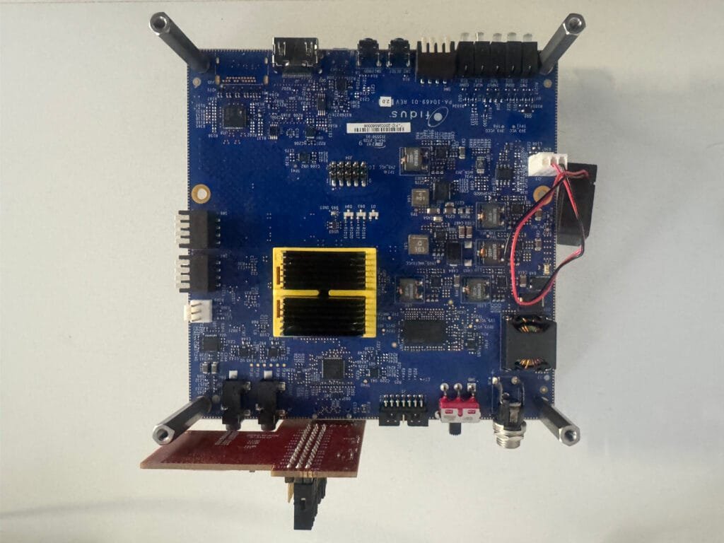
With electronics becoming faster, smaller, and more complex, PCBAs require more power and this occasionally raises their operating temperature. Designing the PCB with an effective thermal performance is a critical factor, as more than half of all electronic components fail due to heat stress, a mismatch of CTE, or heat-induced material degradation. Some best practices we follow to address thermal considerations are:

Thermal Considerations
Best Practices
Excessive warpage of components and PCB.
Ensure adequate spacing between high-power components to manage heat distribution effectively.
Overloading and fatigue of components and solder joints.

Use thicker copper foil in PCB layer stacking or incorporate thermal vias for better heat dissipation.

Long-term degradation of material or components.
Balance copper distribution across top and bottom layers during the design phase to minimize thermal stress.
Distortion due to non-uniform heating.
Select PCB lamination materials with a lower coefficient of thermal expansion (CTE) mismatch.

Heat generation from high-power components.

Conduct computational simulations to analyze thermal behavior before finalizing the PCBA design.

FAQs

PCB reliability testing ensures durability under environmental, electrical, and mechanical stress. It includes:

 Functionality Tests

  • Visual Inspection: Detects physical defects.
  • In-Circuit & Flying Probe Testing: Verifies electrical performance.
  • Automated Optical & X-Ray Inspection: Identifies soldering and internal flaws.
  • Burn-In & Functional Testing: Assesses long-term performance.

 Reliability Tests

  • Environmental & Electrical Stress: Tests extreme conditions.
  • Chemical & Contaminant Resistance: Ensures durability.
  • Radiation Resistance & Artificial Aging: Simulates real-world lifespan.

This ensures PCBs meet quality standards for reliable performance.

PCB failure analysis is the process of identifying and understanding the causes of failures. Failures can occur gradually, intermittently, or suddenly, and each case requires detailed investigation to determine the root cause.

Common PCB defects include:

  • Mechanical Issues: Scratches, dents, and cracks.
  • Dimensional Errors: Inaccurate board measurements.
  • Soldering Problems: Voids, bridging, and cold solder joints.
  • Contamination: Oils, flux residues, and debris.
  • Plating Defects: Thin deposits, nodules, and uneven surfaces.
  • Layer Misalignment: Misaligned inner layers.

Drilling Errors: Poor hole quality and breakouts.

During manufacturing, PCBs can experience:

  • Scratches, dents, cracks, chipping, warpage, and hole defects.
  • These damages often result from mishandling, fixture contact, bending stresses, abrasion, or impacts.

Yes, PCBs can become contaminated during production due to:

  • Dust and debris.
  • Chemical solutions like plating baths and etchants.
  • Metal particles, fingerprints, and flux residues.

ASK US!

Get instant support from our dedicated live customer service team!
logo-iso
ul-logo