


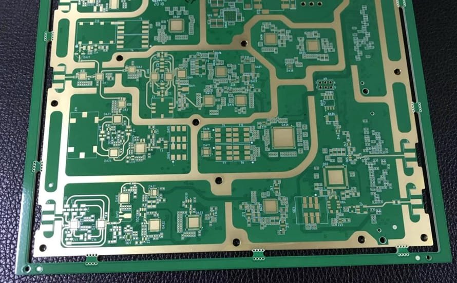
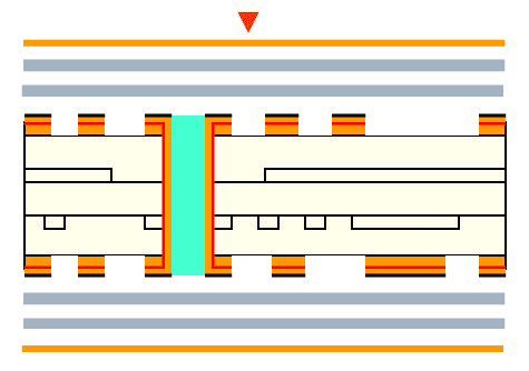
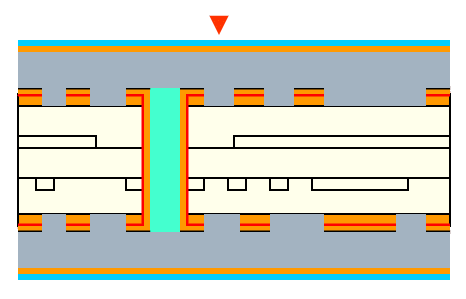
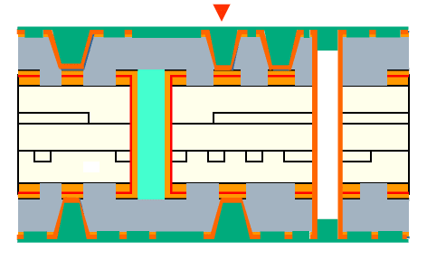
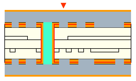
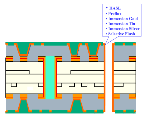
| Prepreg | RCC | |
|---|---|---|
Low Cost | ++ | - |
Strength | ++ | + |
Hole wall roughness | - | + |
Laminating control | + | - |
Dielectric thickness | 45um ~ | 30um ~ 80um |
Smear residue on target pad | - | ++ |
Dielectric constant | 3.9 ~ 4.7 | 3.2 ~ 3.8 |
Shelf time | ++ | + |
Working PNL size | ++ | + |
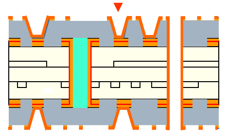
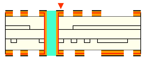
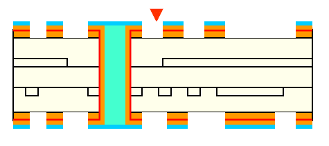
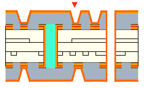
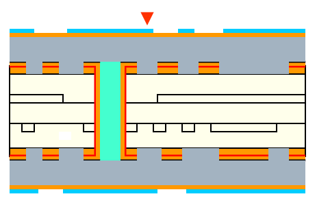
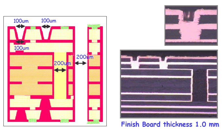
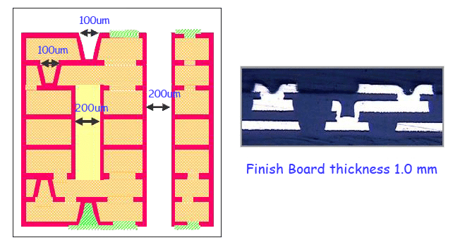
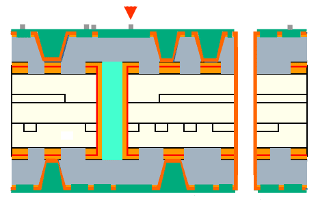
| Mechanical Drilling | Laser Drilling | |
|---|---|---|
Low Cost in Equipment | ++ | + |
Low Cost in Production | + | ++ |
Required Facilities | Drilling Machine | Laser Machine |
Consumable | Drill Bits, Backup Board | None |
Aspect Ratio | 9 | 1 |
Via Size Capacity | 200 um~ | 50~100um |
Speed | 140 H/min | 20,000 H/min |
Throughput | - | + |


© All Copyright 2025 by streampcb.com